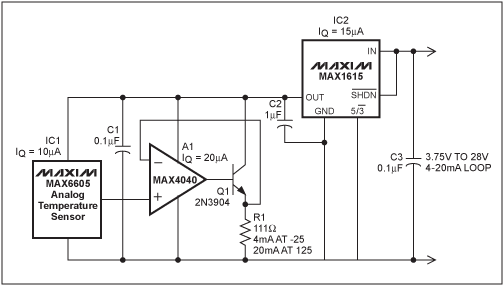
This circuit uses an analog temperature sensor, op amp, transistor, and low-dropout linear regulator to provide a 4mA–20mA output over a 3.75V–28V compliance range. The low quiescent current of the devices used permits them to be powered by the loop with the only consequence being a slight offset error.

Figure 1.
The temperature sensor IC1 feeds the op amp/transistor combinaTIon, A1 and Q1, with R1 as the load on the amplifier. IC1's output consists of an offset of 744mV at 0°C and a scale factor of 11.9mV/°C. R1 is selected to provide the best possible fit of the temperature range of IC1 to the 4mA–20mA output. In this example, IC1's output at -25°C is 0.4465V, and a 111Ω resistor for R1 provides a 4mA output at -25°C. At 125°C IC1's output is 2.213V, yielding 19.937mA with the 111Ω resistor used for R1. This current is reflected at the input of the low-dropout linear regulator IC2.
Besides regulaTIng the voltage to the sensor and op amp circuit, IC2 provides the compliance at the voltage input required for connecTIon to the 4mA–20mA loop. IC2 is pin programmable to provide either 3V or 5V output, and in this circuit is programmed to provide 3V to IC1 and A1. This maximizes the input compliance by allowing input voltages as low as 3.75V (as well as resulTIng in a slight reduction of quiescent current of IC1 and A1, therefore less error due to quiescent current).
Quiescent currents of all components combine and add to the 4mA output which corresponds to negative full scale. Consider this 45µA current in light of the scale factor, which is proportional t
4mA–20mA Output Current Scale Factor = (11.9mV/°C)/R1
and yields a current scale factor of 106.66µA/°C. The 45mA quiescent current represents an offset of approximately 0.43°C. Since it is an offset it is possible to compensate for it elsewhere (such as in software if the temperature data becomes digitized).
A similar version of this article appeared in the May 7, 2001 issue of Electronic Design magazine.